
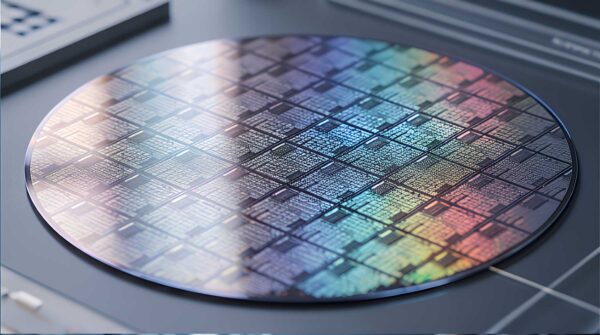
The semiconductor industry demands absolute precision, extreme chemical resistance, and flawless structural stability. When transitioning from machined polymers to semiconductor large custom injection molded parts, engineers frequently question if the injection molding process can achieve and maintain the necessary dimensional tolerances. At EnviroTech, our advanced manufacturing capabilities ensure that massive polymer components meet the exact specifications required for cleanroom environments, fluid handling systems, and wafer processing equipment.
The Challenge of Precision at Scale
Manufacturing large components for semiconductor applications introduces unique engineering challenges. Standard injection molding processes often struggle with material shrinkage, internal voids, and unpredictable warping as the plastic cools. These common defects compromise the dimensional stability of high purity polymer components, rendering them useless for highly sensitive applications where even microscopic variances can lead to system failures, chemical pooling, or contamination.
Achieving Strict Tolerances with Void Free Molding
To meet the strict dimensional requirements of the semiconductor sector, we utilize proprietary Void Free and Thick Wall injection molding techniques. By meticulously controlling the thermal cooling and pressure packing phases for parts weighing up to 580 lbs, we completely eliminate internal cavities and micro porosity. This controlled process guarantees that the internal structure remains completely dense and solid. A void free core prevents structural creep under mechanical stress, ensuring the part holds its exact shape and critical tolerances throughout its lifecycle.
Near Net Shapes and High Purity Materials
Material selection is just as critical as the molding process when engineering semiconductor large custom injection molded parts. We specialize in processing high performance, chemically inert resins like PEEK, PVDF, and PPS. Because these advanced materials are expensive, we employ Near Net Shape molding to form the component as close to its final dimensions as possible. This methodology drastically reduces the need for secondary machining, minimizes costly material waste, and preserves the pristine, untouched surface finish required for high purity polymer components.
Partnering with a Made in the USA manufacturer that understands the extreme demands of the semiconductor industry ensures your supply chain remains resilient and your parts perform flawlessly. By engaging in comprehensive Design for Manufacturing support, we help lock in your critical tolerances early, delivering massive, precision engineered polymer solutions that outperform traditional machined alternatives.